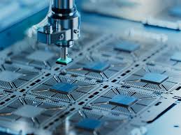
In recent years, advanced packaging has become much more important. While semiconductor manufacturers used to focus primarily on miniaturization and increasing the performance of individual chips, the focus is increasingly shifting to the system level: How can processor cores, memory, sensors, and wireless modules be integrated as efficiently, compactly, and powerfully as possible within a single housing? This is precisely where advanced packaging comes in.
It’s no longer just about so-called chiplets—which involve decomposing complex systems into smaller, specialized functional blocks that are later reassembled. While this idea remains central, the possibilities now extend much further. Advanced packaging enables a new design paradigm that combines mechanical, electrical, thermal, and optical aspects in an integrated system concept. This enables engineers to make complex systems not only more powerful but also more energy-efficient and reliable.
More than chiplets – new forms of integration
Modern packaging technologies aim to condense functionality and shorten signal paths without compromising performance or reliability. Techniques such as through-silicon vias (TSVs), 2.5D interposers, and fan-out wafer-level packaging allow several active chips to be integrated close together or even on top of each other. The components are then connected at the silicon or substrate level, almost as if they were inside a monolith.
Tight coupling of this sort opens up new possibilities for power supply, heat dissipation, and high-speed communication between functional units. This is especially relevant when combining different technologies—such as logic, memory, and sensors—into one package, because it leads to high-performance, heterogeneous systems that take up almost no space at all. At the same time, engineers benefit from a reduction in cabling, which minimizes signal loss and speeds up data transmission.